

TOF Chip and Packaging Advances Driving 3D Sensing to Millimeter Era
With the rapid development of AI, IoT, autonomous driving, and robotics, 3D sensing technology is moving from labs to consumer and industrial applications. Especially, Time-of-Flight (TOF) based 3D sensors, featuring high accuracy, low power, and small size, are becoming the core of 3D vision systems. Continuous progress in TOF chips and packaging is accelerating 3D sensing into the 'millimeter era,' bringing unprecedented spatial perception capabilities to various devices.
What is 3D Vision?
3D vision means acquiring and processing three-dimensional spatial information of objects, enabling computers or machines to perceive, understand, and reconstruct real-world structures. Simply put, 3D vision allows devices not only to 'see' 2D images but also to 'sense' depth, height, and width, realizing spatial perception.
3D vision is widely used in robot navigation, autonomous driving, industrial inspection, virtual reality (VR), augmented reality (AR), etc., using methods like stereo vision, LiDAR, structured light, and TOF cameras.
In short, 3D vision equips machines with the ability to 'see' the world in three dimensions, a core technology driving intelligent manufacturing and automation.

1. TOF Core Hardware Architecture: Transmitter, Receiver, and Chip Collaboration
TOF sensors actively measure distance by emitting modulated light (usually infrared laser or LED) and receiving the reflected light from the target, calculating the round-trip time of the light to obtain accurate distance. This method, based on light speed travel time, provides fast, precise 3D depth sensing, widely applied in robot 3D vision, 3D SLAM, 3D machine vision, and AGV autonomous navigation.
A complete TOF hardware system includes three key parts:
-
Transmitter (TX)
Emits modulated light, commonly infrared VCSEL lasers or high-brightness LEDs. Modulation frequency and power affect measurement accuracy and range. Advances in semiconductor lasers shrink size, lower power, and increase reliability, enabling lightweight, compact TOF modules. -
Receiver (RX)
Captures reflected light, often using sensitive photodetectors like avalanche photodiodes (APD) or single-photon avalanche diodes (SPAD). It requires fast response and high signal-to-noise ratio to detect weak reflections accurately, especially in complex environments. -
Time-to-Digital Converter (TDC)
Converts flight time to digital signals for precise calculation. High-performance TDC chips achieve nanosecond or even picosecond resolution, critical for millimeter or sub-millimeter depth measurements. Leading TDC chips such as GP22, TDC-GPX2 LVDS, TDC-2 HIRES are widely used in high-end 3D TOF cameras and depth sensors.
Integration and synergy among these components on chip level, supported by CMOS advances, enable compact, cost-effective, and fast-response TOF modules.
The mainstream Dtof (Direct TOF) solution directly measures light pulse travel time, avoiding indirect measurement errors, achieving higher accuracy and speed, essential for high-precision applications like robot navigation, autonomous driving, and industrial inspection.
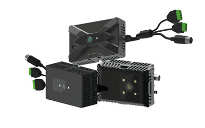
2. CMOS Integration and SiP Packaging: Trends of Miniaturization and Low Power
TOF systems evolve toward higher integration. CMOS-based TOF chips improve sensitivity and response speed while reducing costs for mass production. SiP (System-in-Package) technology integrates lasers, receivers, lenses, control ICs, and TDC chips into a single module, saving PCB space, enhancing interference resistance and heat dissipation.
For example, TOF 3D camera modules with SiP are widely used in 3D smartphone front cameras, smart locks, robot obstacle avoidance, and face recognition.
3. Lightweight TOF Design for Mobile and IoT Devices
With the rise of mobile and IoT devices, demand for compact, low-power, highly integrated sensors grows. Traditional large TOF sensors cannot meet strict size, power, and cost requirements, pushing development of lightweight TOF micro-modules.
These micro-modules have very small sensor areas (<10mm²), high integration, and support RGBD (RGB color + Depth) data capture and output, enabling richer and more accurate spatial perception and interaction.
Advantages include:
-
Compact size, easy integration
Fits smartphones, tablets, wearables, and IoT devices, enabling seamless integration with cameras and chips, reducing device thickness and increasing design flexibility. -
Low power consumption, extended battery life
Advanced power management and low-power chips maintain accuracy and speed while minimizing energy use for long-term operation. -
High integration and multifunctionality
Combines TOF ranging, RGB capture, and digital processing, simplifying design and enhancing stability and performance. -
Multi-scenario applications empowering intelligent interaction
Enables AR overlays, natural gesture recognition, indoor navigation, and 3D scanning.
Also used in lightweight professional 3D vision systems:
-
3D SLAM navigation for real-time environment reconstruction and localization in robots, drones, and AR devices.
-
AGV autonomous navigation with accurate depth data for efficient path planning and obstacle avoidance, improving logistics automation.
-
Smart surveillance (3D CCTV) for precise human action and anomaly detection, enhancing security.
Looking ahead, lightweight TOF technology will drive innovation in robot 3D vision, autonomous industrial robots, and guided robotics, providing accurate 3D perception and real-time interaction, becoming core sensing units for flexible, efficient, intelligent robotics.
With small size, low power, and high integration, lightweight TOF perfectly meets mobile and IoT needs, empowering smart interaction and automation, driving next-generation smart hardware upgrades.

4. Global Supply Chain Trends and the Rise of Domestic TOF Chips
In recent years, the global supply chain environment has become increasingly complex, influenced by geopolitical tensions, trade frictions, and the pandemic, among other factors. The international chip supply chain faces many uncertainties and risks.
The traditional TOF chip market, dominated by European, American, Japanese, and South Korean manufacturers, has gradually revealed problems such as high dependency on foreign suppliers and fragile supply chains. In response to this situation, domestic TOF chip manufacturers have ushered in unprecedented development opportunities, rapidly rising and beginning to break the foreign monopoly, driving China’s TOF industry chain toward independent control and innovative breakthroughs.
On one hand, domestic chip design companies have focused on tackling the core technologies of TOF sensors, making significant progress in key areas such as improving the precision of time-to-digital converters (TDC), optimizing circuit integration, and controlling system power consumption. Multiple Chinese companies have successfully launched TOF chip products with performance comparable to leading international brands, featuring nanosecond-level time measurement capabilities and high-precision distance sensing. These chips not only meet the demanding requirements of traditional industrial and consumer electronics deep sensing but also expand into more diverse application scenarios.
On the other hand, domestic TOF chips are widely applied across fields including smart locks, smart home security, smartphones and tablets, automotive driver assistance, 3D machine vision, and robot navigation. Particularly in the smart lock sector, domestic TOF chips significantly enhance security and user interaction experience by providing high-precision gesture recognition and spatial perception capabilities. In smartphones, combined with RGBD camera technology, they enable face recognition, AR augmented reality, and photo depth-of-field optimization, helping domestic brands boost product competitiveness.
At the same time, with the continuous rise in domestic market demand for high-precision ranging sensors (TOF 3D sensors) and RGBD cameras, domestic TOF chip companies have gained broad development space. The digital transformation and intelligent upgrades in various industries have driven strong demand for depth sensing technology, especially in intelligent manufacturing, smart cities, autonomous driving, and logistics warehouse automation, where the need for high-performance TOF solutions is increasingly urgent. This provides a solid market foundation and growth momentum for domestic chip manufacturers.
Additionally, domestic government and industry alliances have provided strong policy support and funding for semiconductor independent innovation and local supply chain construction. Relying on abundant R&D resources and an innovative ecosystem, domestic TOF chip companies actively promote improvements in key materials, design tools, and testing and verification systems, accelerating the establishment of a full industry chain from chip design to module integration and system solutions.
In the future, as technology matures and scale effects increase, domestic TOF chips will continue to improve performance and reduce costs, further expanding market share. The rise of domestic manufacturers will not only help strengthen China’s voice in the global 3D sensing field but also promote the entire industry toward a more open and win-win ecosystem. Through technological innovation and supply chain optimization, domestic TOF chips are becoming a key force leading the new era of intelligent visual perception, injecting strong momentum into global smart hardware and IoT applications.

5. New Materials and Packaging Technologies Enhancing TOF Performance
Entering the 'millimeter era' of TOF sensing, new materials and advanced packaging technologies have become key drivers for improving TOF sensor performance. As application demands become more diversified and high precision requirements rise, traditional materials and processes increasingly struggle to meet challenges in optical efficiency, thermal stability, and size integration of TOF systems. The introduction of innovative materials and precision packaging technologies significantly enhances the overall performance and reliability of TOF sensors, promoting their widespread use in consumer electronics, industrial automation, intelligent security, and AIoT terminals.
Firstly, the application of micro-lens array (MLA) materials greatly improves the efficiency of light reception. By integrating high-transmittance micro-lens arrays on the receiver surface, reflected light signals are effectively focused and guided, increasing photoelectric conversion efficiency and enhancing detection capabilities under weak light conditions. This not only improves TOF system ranging accuracy but also enhances system stability and anti-interference ability in complex lighting environments.
Secondly, the use of high infrared transmittance glass packaging materials is crucial for reducing optical signal transmission loss. High-quality infrared-transmitting glass minimizes absorption and scattering of light during packaging, ensuring complete transmission of emitted laser and reflected light, thus improving system detection sensitivity and depth resolution. At the same time, these materials have good mechanical strength and environmental resistance, enhancing TOF sensor durability.
Thirdly, the use of low thermal expansion packaging adhesives effectively ensures precise alignment between lasers and receiving sensors. TOF systems require high stability of optical paths, and mismatched thermal expansion of packaging materials easily causes component misalignment, impacting ranging accuracy and imaging consistency. Low thermal expansion adhesives maintain structural stability under temperature changes, ensuring long-term stable operation of TOF modules, especially suitable for industrial and outdoor applications with large temperature fluctuations.
Moreover, wafer-level packaging (WLP) technology achieves high integration and miniaturization of TOF chips and sensor modules, significantly reducing module size and manufacturing costs. WLP enables large-scale deployment of TOF sensors in space-constrained consumer smart devices and AIoT terminals, such as smartphones, smart speakers, and smart cameras, promoting the popularization and innovative application of 3D sensing technology in the mass market.
Furthermore, as integration of multiple sensing technologies becomes a trend, TOF sensors are increasingly deployed alongside laser TOF sensors, ultrasonic airflow measurement, infrared level detectors, and other types of sensors. Through heterogeneous sensor fusion, 3D sensing systems not only enhance spatial perception accuracy and environmental adaptability but also achieve functional complementarity and data fusion, greatly improving intelligent terminals’ perception ability and smart response in complex environments.
In summary, breakthroughs in new materials and packaging processes drive TOF sensor performance improvement from a single dimension to comprehensive indicators. In the future, with continuous progress in material science and packaging technology, TOF systems will achieve qualitative leaps in resolution, response speed, stability, and power consumption, providing more precise and efficient 3D sensing solutions for intelligent vision, robot navigation, industrial inspection, and smart city applications.
Conclusion: TOF Chip Innovation Leading the 3D Sensing 'Millimeter Era'
It is foreseeable that, with the continuous advancement of semiconductors 2024 new trends and the ongoing enhancement of 3D TOF camera chip performance, TOF technology will deeply integrate with visual SLAM, AI perception systems, and 3D robotics platforms, unleashing greater potential in fields such as intelligent security, industrial automation, autonomous driving, intelligent warehousing, and human-computer interaction.
We are standing at a critical node in the evolution of 3D sensing technology. Every iteration of TOF chips and packaging technology is paving the way toward a 'millimeter-level' future.
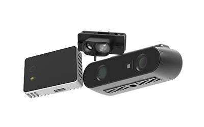
Synexens 3D Camera Of ToF Sensor Soild-State Lidar_CS20

After-sales Support:
Our professional technical team specializing in 3D camera ranging is ready to assist you at any time. Whether you encounter any issues with your TOF camera after purchase or need clarification on TOF technology, feel free to contact us anytime. We are committed to providing high-quality technical after-sales service and user experience, ensuring your peace of mind in both shopping and using our products