

Electron Microscope Advantages Over Light Microscopes & TOF Integration
In scientific research, microscopes are widely used in various fields, from biology to material science, with different types of microscopes offering powerful analytical tools for researchers. Among these, the electron microscope (EM) has significant advantages over the traditional light microscope (LM), especially in observing fine structures and providing high-resolution imaging.
This article explores the advantages of electron microscopes compared to light microscopes and showcases how Time-of-Flight (TOF) technology, when combined with electron microscopes, is driving the frontier of scientific research.
What is an Electron Microscope Used For?
Applications of the Electron Microscope
An electron microscope is a high-resolution microscope that uses an electron beam instead of visible light for imaging. It can observe and analyze the microscopic structure of samples and is widely used in various fields. The primary applications include:
-
Material Science
Electron microscopes are used to observe the microstructure of materials such as metals, ceramics, and polymers, examining their crystal structure, surface defects, and interface characteristics. In nanotechnology, it is a critical tool for studying nanomaterials and nanostructures. -
Biological Research
In biology, electron microscopes help study the structure of cells, organelles, viruses, and bacteria. By observing the fine details of cells (such as the cell membrane, endoplasmic reticulum, and mitochondria), researchers can gain deeper insights into cell functions and biological processes. -
Medical Diagnostics
Electron microscopes are used in pathology, particularly in cancer research, by examining the ultrastructure of diseased cells for early disease detection. It is also employed in neuroscience to study the connections between neurons and the structure of neural networks. -
Semiconductor Industry
Electron microscopes are used in the semiconductor industry to analyze the microstructure of chips, detect defects, and study transistor performance. In manufacturing and quality control, it is an indispensable tool. -
Nanotechnology
In nanotechnology, electron microscopes are used to observe and analyze nanoscale objects, helping researchers study nanoparticles, nanomaterials, and their applications. -
Chemical Analysis
Electron microscopes, when coupled with energy dispersive spectroscopy (EDS), can perform elemental composition analysis, allowing researchers to understand the chemical makeup of materials.
The electron microscope, with its ultra-high resolution and precise detail-rendering capabilities, plays a crucial role in many scientific fields.

Advantages of Electron Microscopes Over Light Microscopes
-
Higher Resolution
The resolution of light microscopes is limited by the wavelength of light and can typically resolve to about 0.2 microns. Electron microscopes, using electron beams as an imaging source, achieve much shorter wavelengths than light, enabling them to resolve structures at the nanometer scale (about 0.1 nanometers). This ultra-high resolution allows electron microscopes to clearly observe cellular structures, viruses, and even atomic-level features, far exceeding the capabilities of light microscopes. -
More Precise Detail Presentation
Electron microscopes can present internal structures and surface features of objects. Whether it's organelles within a cell or microcracks on a material’s surface, electron microscopes can capture these details with exceptional clarity, making them irreplaceable in fields like material science, nanotechnology, and biomedicine. -
3D Imaging Capability
Modern electron microscopes, in addition to standard 2D imaging, can provide three-dimensional imaging through scanning or transmission electron microscopy (SEM, TEM). This capability helps researchers better understand the spatial structure of samples, something light microscopes cannot provide. -
Surface Analysis
Electron microscopes can not only image internal structures but also perform surface analysis through additional detectors like Energy Dispersive Spectroscopy (EDS), which provides chemical composition information of the sample. This makes electron microscopes particularly valuable in material analysis and chemical research, a feature light microscopes lack.
The Integration of Electron Microscopes with TOF Technology
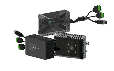
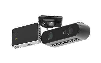
Time-of-Flight (TOF) technology is a technique that measures the time difference between the emission and reception of light or other signals to determine distance. This technology has been widely used in applications like LiDAR (Light Detection and Ranging), depth cameras, and drone obstacle avoidance. TOF technology, known for its high precision and fast response, provides real-time depth data in various scenarios. When integrated with electron microscopes, TOF technology significantly expands the applications of electron microscopy, offering richer and more precise information, particularly in 3D imaging, surface analysis, and real-time data acquisition.
1. TOF Technology Enhancing Electron Microscope 3D Imaging
Electron microscopes capture high-resolution 2D images of samples through electron beam scanning, but traditional electron microscopes are limited in providing depth information. The introduction of TOF technology can bridge this gap, helping researchers not only obtain surface details but also gain spatial depth data. By measuring the time delay of electrons or light signals reflected back from the sample, TOF technology calculates the distance of different areas, generating 3D imaging data. This is crucial for analyzing the 3D structures of complex biological tissues, nanomaterials, and microdevices, providing a more comprehensive understanding of the sample’s microscopic structure and properties.
For example, in biological tissue analysis, electron microscopes can clearly observe cell details, while combining TOF technology allows researchers to obtain depth data, enabling a more accurate analysis of cellular 3D shapes and understanding their function and pathological changes.
2. Improved Imaging Speed and Accuracy
One of the advantages of TOF technology is its efficient real-time data collection capability, which is particularly valuable in electron microscopy applications. Traditional electron microscopes are slow in scanning large samples or performing long-term observations, which can lead to imaging delays and errors. TOF technology, by quickly measuring signal flight times, accelerates the imaging process, reducing errors and improving measurement accuracy. The integration of TOF with electron microscopes can significantly enhance imaging efficiency, especially when scanning large areas, producing high-resolution images and 3D structure analyses in a shorter time.
This is particularly useful for large-scale sample studies, such as thin film samples in material science or tissue sections in biological studies, providing more efficient and precise analysis.
3. TOF Technology in Biomedical Applications
The integration of TOF technology with electron microscopes has shown great potential in biomedical research, especially in early disease detection and diagnostics. In cancer research, electron microscopes provide high-resolution images of tumor cells and their microenvironment, displaying cellular morphology, structure, and growth patterns. TOF technology, on the other hand, allows for precise measurement of shape and size changes, providing additional depth data that aids early cancer cell detection.
For instance, by combining TOF technology, electron microscopes not only show cancer cell morphology but also reveal deep features such as membrane thickness and cytoplasm changes, which help in early cancer screening and precision treatment.
4. Applications in Nanomaterials and Semiconductor Research
In nanotechnology and semiconductor research, the combination of electron microscopes and TOF technology offers significant advantages. Electron microscopes provide nanoscale imaging resolution, allowing researchers to observe fine structures in nanomaterials and devices. By adding TOF technology, researchers can obtain precise 3D measurements of materials' shapes, thicknesses, and depths.
In the semiconductor industry, the integration of electron microscopes and TOF technology is crucial. Surface defects in semiconductor chips may affect their performance, and traditional electron microscopes only display surface details. TOF technology can help detect internal structural changes such as microcracks or pores, enabling engineers to optimize production processes and improve chip quality and performance. For example, TOF can measure thickness variations between layers and surface depth changes, aiding in quality control and defect analysis in semiconductor manufacturing.
In nanomaterials development, TOF technology combined with electron microscopes helps researchers obtain more accurate 3D structural information, advancing the design and application of high-performance electronic devices, optical materials, and other advanced research areas.

Conclusion
Electron microscopes play a vital role in modern scientific research with their ultra-high resolution, precise detail presentation, and powerful 3D imaging capabilities. The integration of Time-of-Flight (TOF) technology further enhances the capabilities of electron microscopes in spatial analysis and precise measurement. This combination not only improves the accuracy of imaging but also drives breakthroughs in fields like biomedicine, material science, nanotechnology, and semiconductor research.
As TOF technology continues to advance, the future of electron microscopes will evolve from being static observation tools to intelligent, precise analytical platforms. Whether in biological research revealing the secrets of cells or in optimizing material performance for semiconductor chips, the synergy between electron microscopes and TOF technology will undoubtedly continue to push the boundaries of scientific research and technological innovation, leading to more discoveries and innovations.
Synexens 3D Of RGBD ToF Depth Sensor_CS30

Our professional technical team specializing in 3D camera ranging is ready to assist you at any time. Whether you encounter any issues with your TOF camera after purchase or need clarification on TOF technology, feel free to contact us anytime. We are committed to providing high-quality technical after-sales service and user experience, ensuring your peace of mind in both shopping and using our products.
-
Publicado en
CS30