Electron Microscopy Meets ToF: Advancing Nanotech, Materials Science

What is Electron Microscopy Used For?
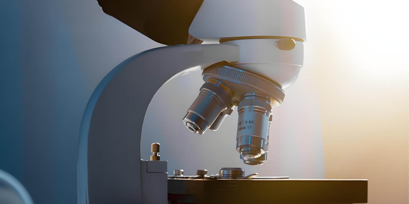
With advancements in technology, the integration of Electron Microscopy (EM) with Time-of-Flight (ToF) technology is fostering innovations in nanotechnology, material science, and other research fields. As a high-resolution imaging method, electron microscopy captures microscopic and even atomic-level structures, while ToF technology excels in precise spatial information and distance measurement. Together, these technologies enable researchers to achieve enhanced accuracy and obtain more comprehensive experimental data and insights.
1. Electron Microscopy: A Core Tool for Exploring the Microscopic World
Electron microscopy employs electron beams instead of light to achieve much higher resolutions, enabling the observation of minute structures. Common types of electron microscopy include Scanning Electron Microscopy (SEM) and Transmission Electron Microscopy (TEM), widely applied in material science, biomedicine, nanotechnology, and semiconductor industries.
By using electron microscopy, researchers can deeply analyze the surface and internal structures of materials, revealing their microscopic composition and physical properties. However, traditional electron microscopes primarily capture two-dimensional images, lacking depth information—a limitation that ToF technology effectively overcomes.
2. Time-of-Flight (ToF) Technology: A New Era of Depth Perception
Time-of-Flight (ToF) technology measures the time taken for light to travel from emission to return, enabling highly accurate distance calculations and depth imaging. Widely applied in drones, robotics, and autonomous vehicles, ToF technology provides precise spatial data and creates detailed three-dimensional models of objects.
Unlike traditional 2D imaging, ToF's depth perception capabilities offer comprehensive spatial information, making it a key tool for many high-precision measurement and imaging tasks.
3. Combining Electron Microscopy and ToF Technology: A New Perspective
The integration of Electron Microscopy (EM) and Time-of-Flight (ToF) technology has brought revolutionary changes to microscopic research. Their synergy not only surpasses the limitations of traditional methods but also significantly enhances measurement precision and data analysis capabilities.
In nanotechnology research, traditional electron microscopes are renowned for their high-resolution 2D imaging of surfaces, capable of revealing microscopic and even atomic details. However, their inability to provide depth information limits a comprehensive understanding of an object's three-dimensional structure.
With the incorporation of ToF technology, this limitation is addressed. By leveraging ToF's precise depth measurement capabilities, electron microscopes gain powerful 3D perception. Researchers can use this depth data for more accurate 3D reconstructions, revealing not only surface features but also microscopic spatial forms and internal structures.
Enhanced Research Applications
-
3D Morphology Analysis
In material science, analyzing the three-dimensional morphology of materials is crucial for understanding their performance. For instance, the distribution of voids, cracks, and nanoparticles in composite materials directly affects their strength and conductivity. With ToF technology, electron microscopes can capture these key spatial features, providing comprehensive data for optimizing material design. -
Monitoring Dynamic Structural Changes
Traditionally, electron microscopes were primarily used for static observations. By introducing ToF technology, researchers can construct dynamic 3D models from multiple frames of depth information. This is particularly critical for studying how internal structures respond to external conditions, such as temperature, pressure, or electric fields. For example, in semiconductor device research, ToF-enhanced electron microscopy can accurately track how nanoscale stress impacts crystal structures. -
Defect Localization and Characterization
Detecting microscopic defects is essential in nanotechnology and industrial manufacturing. The combination of ToF and electron microscopy enables comprehensive sample scanning to precisely locate internal cracks, voids, or inclusions. This approach overcomes the limitations of traditional 2D imaging in terms of perspective and resolution, providing more efficient and intuitive defect characterization. -
3D Imaging in Biology and Medicine
Biological tissues and cellular structures are inherently complex and three-dimensional, making it challenging to capture their true morphology with traditional 2D imaging. By integrating ToF technology, electron microscopes can reconstruct clear 3D models of cells, aiding in the analysis of dynamic processes such as cell division and organ development. This provides new tools for medical diagnostics and therapeutic research.
Improved Measurement Precision and Data Analysis
This combination not only enhances spatial resolution and depth accuracy but also provides multidimensional data for analysis. Using depth maps generated by ToF sensors, researchers can create detailed multidimensional models that combine 2D microscopic imaging with 3D depth data. This approach offers novel solutions for complex research challenges.
For instance, multi-scale analysis in material science can be achieved by integrating microscopic 2D surface imaging with macroscopic 3D structural data, significantly boosting the overall effectiveness of research.
4. Applications of ToF-Enhanced Electron Microscopy
-
Semiconductor Research and Manufacturing
In the semiconductor industry, electron microscopes are used to examine microstructures in chips. ToF technology further assists in accurately measuring surface irregularities and detecting tiny defects, significantly enhancing the quality control process in chip manufacturing. -
Nanomaterial Analysis
Studying nanomaterials often requires meticulous observation of their surface and internal structures. ToF-enhanced electron microscopy can provide complete 3D images, helping researchers better understand the properties and potential of nanomaterials, driving the development of innovative materials. -
Biomedical Research
In the biomedical field, ToF-enhanced electron microscopy allows for the examination of three-dimensional structures in cells and tissues, offering more precise insights for early disease diagnosis and treatment planning.
5. Future Prospects
As ToF and electron microscopy technologies continue to advance and integrate, we can expect more innovative applications to emerge. This combination not only enhances nanoscale measurement precision but also has the potential to revolutionize fields like non-destructive testing and precision manufacturing. Scientists are exploring how these technologies can enable more efficient automated analysis and even real-time monitoring.
In the future, with the addition of artificial intelligence and big data, ToF-enhanced electron microscopy will become a core tool in many industries, driving scientific research and industrial production to new heights.
Conclusion
The integration of electron microscopy and Time-of-Flight (ToF) technology represents the future of microscopic exploration. By combining the strengths of both, researchers can acquire more comprehensive and precise microscopic and 3D spatial information, driving technological innovation across various fields. As these technologies mature, ToF-enhanced electron microscopy will play an increasingly vital role in scientific research, medical diagnostics, engineering, and manufacturing.
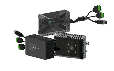
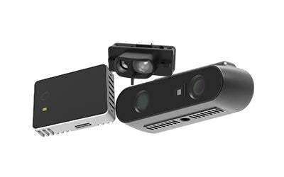
Synexens 3D Of RGBD ToF Depth Sensor_CS30
Our professional technical team specializing in 3D camera ranging is ready to assist you at any time. Whether you encounter any issues with your TOF camera after purchase or need clarification on TOF technology, feel free to contact us anytime. We are committed to providing high-quality technical after-sales service and user experience, ensuring your peace of mind in both shopping and using our products
-
Posted in
CS30


