

How Semiconductor Chips Enhance TOF Technology in Smart Devices
How Semiconductor Chips Drive the Development of TOF Technology?
In today’s smart technology era, semiconductor chips have become a core component of smartphones, autonomous driving, robotics, augmented reality (AR), virtual reality (VR), and other high-tech products. TOF (Time of Flight) technology, an important tool for 3D depth perception, is widely used in 3D facial recognition, LiDAR (Light Detection and Ranging), smart security, drone mapping, and many other fields.
So, what role do semiconductor chips play in TOF technology? How do they enhance depth perception, precision measurement, and data processing capabilities? This article will delve into the relationship between semiconductor chips and TOF technology, as well as their development trends in the future.
1. What Does a Semiconductor Do?
Basic Principles of Semiconductor Chips
A semiconductor chip is an electronic component made from materials like silicon (Si), silicon carbide (SiC), gallium arsenide (GaAs). What makes it unique is its ability to behave as either a conductor or insulator under different conditions, making it a key component for controlling electronic signals.
Main Functions of Semiconductor Chips
The core functions of semiconductor chips include:
- Signal processing: Used for computing and controlling smart devices like smartphones, computers, and artificial intelligence (AI) chips.
- Data storage: Widely used in flash memory (NAND), dynamic random access memory (DRAM), etc.
- Power management: Optimizes energy consumption in electronic devices to improve battery life.
- Sensing and measurement: Used in cameras, LiDAR, TOF sensors, and other depth measurement applications.

2. What is TOF Technology? How Does It Rely on Semiconductor Chips?
Working Principle of TOF (Time of Flight) Technology
TOF (Time of Flight) is a 3D sensing technology based on optical distance measurement. Its basic principle is:
- The device emits a laser pulse or infrared light.
- The light reflects back to the sensor after hitting an object.
- The time of flight (ToF) of the light is calculated, thereby measuring the object’s distance and depth information.
Key Semiconductor Components in TOF Sensors
To achieve high-precision TOF measurements, sensors use various semiconductor chips:
- VCSEL (Vertical Cavity Surface Emitting Laser) chips: Emit high-power, stable laser pulses.
- CMOS/CCD image sensor chips: Capture the reflected light and convert it into an electrical signal for processing.
- SPAD (Single Photon Avalanche Diode) chips: Enhance photon detection capability in low light environments, ensuring measurement precision.
- Signal processing chips (ASIC or FPGA): Used to calculate the time of flight and convert it into depth information.
Breakthroughs in Semiconductor Technology in TOF Sensors
The performance enhancement of modern TOF sensors is driven by advanced semiconductor processes, with breakthroughs in several key areas that make them more advantageous in applications such as smart devices, autonomous driving, industrial inspection, and smart cities.
🔹 Ultra-High Precision Distance Measurement: TOF sensors depend on high-speed VCSEL laser emitters and high-sensitivity SPADs, providing millimeter-level or even micrometer-level precision. Whether in 3D facial recognition, augmented reality (AR), robotic vision, or precision industrial measurements, medical imaging, they ensure precise depth and shape information capture.
🔹 High-Speed Data Processing: Traditional TOF systems require a lot of light signal processing and time calculations. With advancements in semiconductor technology, AI-accelerated computing chips (such as NPUs and DSPs) can process millions of depth data points in real-time, achieving smoother 3D perception. In fields like autonomous driving, smart security, and industrial automation, high-speed data processing ensures systems respond quickly, avoiding security risks caused by delays.
🔹 Low Power Consumption and High Integration: As semiconductor processes evolve from 10nm, 7nm to 5nm and 3nm, the power consumption of TOF sensor chips is drastically reduced, while their size is smaller, enabling integration into smartphones, wearables (AR glasses), drones, and robots. More efficient power management chips (PMIC) and lower-power VCSEL lasers allow TOF technology to maintain high precision while providing longer battery life, enhancing user experience in mobile devices.
🔹 Environmental Adaptability and Multi-Scene Applications: Advanced semiconductor materials like silicon carbide (SiC) and gallium nitride (GaN) are enhancing the stability of TOF sensors in complex environments (strong light, low light, smoke, rain, and snow). This breakthrough allows TOF technology to maintain precise measurements in extreme conditions like nighttime autonomous driving, drone mapping, smart monitoring, and medical 3D scanning, providing more intelligent and reliable solutions for various industries.
With continuous advancements in semiconductor technology, TOF sensor performance in terms of distance precision, calculation speed, power consumption, and environmental adaptability will further improve, providing strong technical support for the development of the smart world.

3. Core Applications of Semiconductor Chips and TOF
(1) Smartphones: 3D Facial Recognition and AR Experience
Modern smartphones widely adopt TOF depth sensors for 3D facial recognition (Face ID), gesture control, and augmented reality (AR) applications. The role of semiconductor chips in these applications includes:
🔹 VCSEL laser emitter chips: Used to project infrared light, creating a 3D depth map.
🔹 CMOS/CCD sensor chips: Capture reflected light and calculate facial feature points.
🔹 AI processing chips: Accelerate facial recognition calculations to ensure unlocking speed.
(2) LiDAR and Autonomous Driving
In autonomous vehicles and drone mapping, LiDAR (Light Detection and Ranging) technology relies on high-performance semiconductor chips.
TOF chips support LiDAR ranging**, achieving centimeter-level precision in 3D modeling.
High-power semiconductor lasers are used for long-distance detection, improving the safety of autonomous driving.
(3) Robotics and Smart Security
Service robots, industrial robots, and security monitoring devices use TOF sensors for target recognition, obstacle avoidance, and environmental perception.
Semiconductor image sensor chips enhance recognition capabilities in low-light environments.
FPGA/ASIC chips accelerate 3D data processing, improving robot decision-making speed.
(4) Smart Cities: Drone Mapping and Infrastructure Monitoring
LiDAR-equipped drones (UAVs) can be used for city mapping, bridge inspections, disaster monitoring, and other scenarios.
🔹 TOF sensors + AI chips can quickly generate high-precision 3D maps.
🔹 Low-power semiconductor chips improve drone endurance, enhancing operational efficiency.

4. How Semiconductor Chips Drive the Future Development of TOF Technology
(1) Higher Precision 3D Depth Perception
As 3nm and 2nm chip processes evolve, TOF technology will achieve higher depth resolution, meeting the needs of medical imaging, industrial inspection, and metaverse (Metaverse) applications that require high precision.
(2) Lower Power Consumption and Miniaturized Design
In the future, low-power semiconductor chips will further enhance TOF sensor applications in smart glasses, wearable devices, making them more suitable for daily use.
(3) Faster Data Processing Capabilities
With the integration of AI computing chips, TOF sensors will be able to identify objects and analyze environments faster, providing stronger decision support for autonomous driving and smart security.
Conclusion: Semiconductor Chips are the Core Support for TOF Technology
Semiconductor chips determine the ranging accuracy, power consumption, and data processing capabilities of TOF sensors.
Advanced semiconductor processes will drive the application of TOF technology in smartphones, autonomous driving, robotics, smart cities, and more.
In the future, low-power, high-precision, and highly integrated semiconductor chips will make TOF technology more intelligent, driving the comprehensive upgrade of 3D perception technology.
The combination of semiconductor chips and TOF technology is leading the development of future technology, creating a smarter and more efficient world.
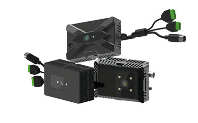
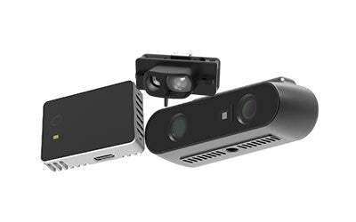
Synexens 3D Of RGBD ToF Depth Sensor_CS30

Our professional technical team specializing in 3D camera ranging is ready to assist you at any time. Whether you encounter any issues with your TOF camera after purchase or need clarification on TOF technology, feel free to contact us anytime. We are committed to providing high-quality technical after-sales service and user experience, ensuring your peace of mind in both shopping and using our products.
-
Posted in
CS30